How to Design Effective EMI/RFI Filters for Power Supplies
💡 Quick Tip
Mastering EMI/RFI filter design is vital for power supply EMC compliance, utilizing common mode chokes, X, and Y capacitors to mitigate conducted emissions effectively.
Introduction
In the realm of modern electronics, where component density and switching speeds continue to escalate, controlling Electromagnetic Interference (EMI) and Radio Frequency Interference (RFI) has become a fundamental pillar in product design. Power supplies, particularly Switched-Mode Power Supplies (SMPS), are notorious noise generators due to their rapid current and voltage transitions. This noise can degrade the performance of other devices, cause functional failures, and even compromise safety. To counteract this, the design of EMI/RFI filters is not optional but a critical requirement to comply with Electromagnetic Compatibility (EMC) standards such as CISPR, FCC, or EN, ensuring that products can coexist seamlessly in an electromagnetic environment.
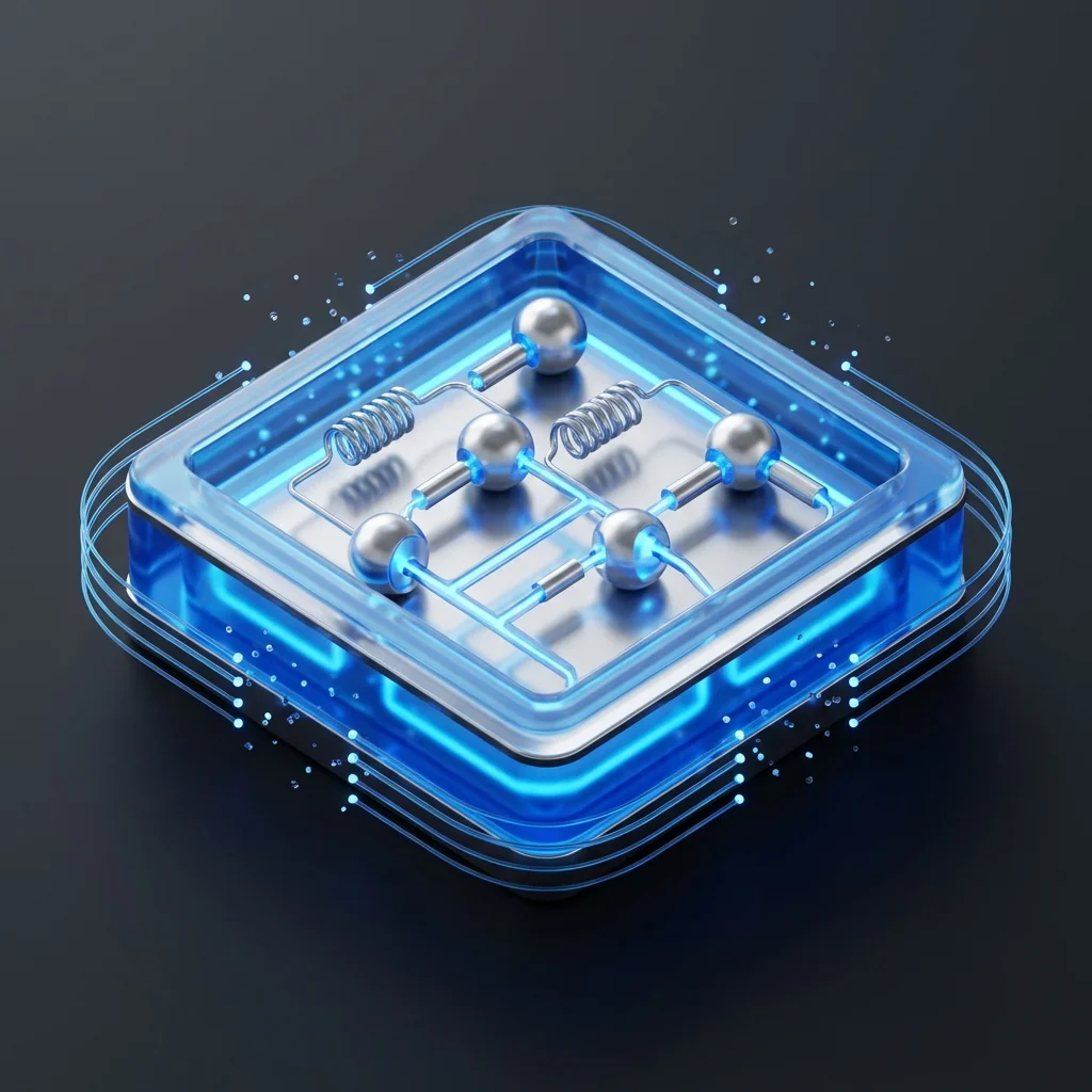
Architecture and Concept of EMI/RFI Filters
Electromagnetic noise in a power supply can primarily be classified into two modes: Differential Mode (DM) and Common Mode (CM).
- Differential Mode (DM) Noise: This is noise that flows in opposite directions between the line and neutral conductors (or positive and negative in DC). It behaves like an undesired load current. It is effectively attenuated with X capacitors (connected between line and neutral) and differential mode chokes.
- Common Mode (CM) Noise: This is noise that flows in the same direction along both conductors (line and neutral) and returns via the ground connection or parasitic capacitance. This type of noise is particularly problematic and propagates efficiently through capacitive and inductive coupling to other parts of the system or the environment. It is primarily mitigated with Common Mode Chokes (CMC) and Y capacitors (connected from line/neutral to ground).
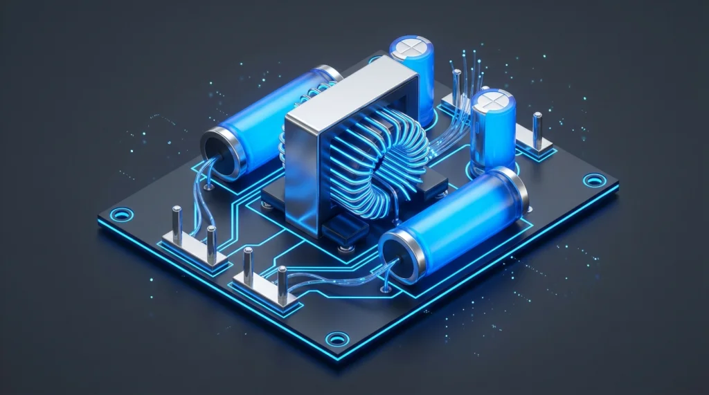
A typical EMI/RFI filter combines these elements. A Common Mode Choke (CMC) consists of two identical windings on the same magnetic core. Differential mode currents magnetically cancel each other in the core, allowing low impedance for the main power signal. However, for common mode currents, the magnetic fields sum up, presenting high impedance that blocks CM noise. Y capacitors complement the CMC by shunting CM noise to ground. On the other hand, X capacitors absorb DM noise. The topology of a filter can be simple (a single L-C stage) or multi-stage (several L-C in series) to achieve greater attenuation over a wider frequency range.
Design Processes and Key Considerations
Designing an EMI/RFI filter is an iterative process that requires a systematic approach:
- Noise Source Characterization: Identify noise sources within the power supply (e.g., switching transistors, recovery diodes, transformers) and their dominant frequency range through conducted emissions measurements.
- Attenuation Requirements Definition: Compare noise measurements with the limits set by applicable EMC regulations. The difference between the measured noise level and the limit defines the required attenuation.
- Component Selection: Choose appropriate inductor (choke) and capacitor values. For CMCs, the inductance value and core material (e.g., ferrites) are critical for the desired frequency range. For Y capacitors, leakage current is a fundamental safety consideration, limited by regulations to prevent electric shock. Rated voltage and current capacity are also important.
- Filter Topology Design: Determine whether a simple or multi-stage approach is needed, and the arrangement (e.g., L, Pi, or T filter) to achieve the desired attenuation. It is crucial that the filter is placed as close as possible to the noise source (the power input point) and that the ground connection offers low impedance.
- Simulation and Prototyping: Utilize simulation tools to predict filter performance and then build a prototype. PCB layout is vital; a poor arrangement can nullify the filter's effectiveness due to parasitic capacitances and inductances.
- Testing and Validation: Conduct conducted emissions tests in an EMC laboratory. This step often reveals the need to adjust component values, topology, or layout.
Additional considerations include choke saturation (which can occur with high load currents or spikes, drastically reducing the effective inductance), component resonance (capacitor ESR/ESL and inductor parasitic C/L), and power dissipation in inductors.
Key Parameters and Future Outlook
The main parameters defining the performance of an EMI/RFI filter are Insertion Loss, input and output impedance, and its behavior with respect to temperature and load variation. Insertion loss is measured in decibels (dB) and represents the attenuation of noise across the filter. To optimize the design, it is fundamental to understand that components have non-ideal characteristics: parasitic capacitance in inductors and parasitic inductance (ESL) and equivalent series resistance (ESR) in capacitors limit their effectiveness at high frequencies.
In the future outlook, filter design will advance towards the integration of more efficient materials, such as nanocrystalline cores that offer higher inductance and lower loss at high frequencies. Active filtering techniques will also be explored as an alternative to passive filters to reduce size and weight, especially in high-power applications. Multi-physics simulation and tools based on artificial intelligence and machine learning will play an increasing role in optimizing design and predicting filter performance, shortening development cycles and improving EMC compliance from the earliest design stages.
📊 Practical Example
Real-World Scenario: EMI Filter Design for a Laptop Power Adapter
Technical Problem: A new 90W AC/DC laptop power adapter prototype, based on a flyback topology, exceeds the conducted emissions limits of CISPR 32 Class B regulations in the 150 kHz to 30 MHz range, particularly with common mode noise peaks around 500 kHz and 5 MHz.
Objective: Design an input EMI/RFI filter to comply with regulations, minimizing cost and size.
Detailed Steps:
-
Initial Analysis and Measurement:
- Conducted emissions measurement is performed in the EMC laboratory without a filter, using a Line Impedance Stabilization Network (LISN). Results show that common mode noise is dominant, with required attenuation of approximately 20 dB at 500 kHz and 30 dB at 5 MHz.
-
Common Mode Component Selection:
- Common Mode Choke (CMC): To cover the range from 500 kHz to 5 MHz and beyond, a CMC with an inductance value of 10 mH is selected. A high-permeability ferrite core is chosen to maintain its effective inductance in the desired frequency range and not saturate at the source's nominal current (approximately 0.4A RMS for 90W at 230VAC). For adapter applications, a compact size is crucial.
- Y Capacitors (CY1, CY2): Two 2.2 nF ceramic capacitors (Class Y1 or Y2 for safety, depending on working voltage) are used, connected from the line and neutral to the chassis safety ground (or to the PCB ground if isolated and certified). This capacitance value is selected to effectively shunt high-frequency noise to ground, keeping the total leakage current below 0.75 mA (a common limit for portable equipment).
-
Differential Mode Component Selection (Optional/Complementary):
- Although CM noise is dominant, there is always a DM component. An X Capacitor (CX1) of 220 nF (Class X2) is added between line and neutral to attenuate any remaining differential noise and input voltage peaks. This value provides low impedance for DM noise but high impedance for the line frequency (50/60 Hz).
-
Filter Topology Design:
- A basic L-C filter configuration is implemented. The CMC is placed in series with the AC input lines, followed by the Y capacitors to ground. The X capacitor is connected in parallel at the CMC input or between the CMC and the rectification, depending on space and layout requirements. A typical configuration would be:
CX1(between L/N) ->CMC(in L and N) ->CY1/CY2(from L/N to Ground).
- A basic L-C filter configuration is implemented. The CMC is placed in series with the AC input lines, followed by the Y capacitors to ground. The X capacitor is connected in parallel at the CMC input or between the CMC and the rectification, depending on space and layout requirements. A typical configuration would be:
-
PCB Layout Considerations:
- The filter is positioned as close as possible to the AC input connector to intercept noise before it propagates across the PCB. Traces between filter components are kept short and wide. The ground connection for the Y capacitors is made to a robust ground plane to ensure a low-impedance path for common mode noise.
- Clear physical separation (a 'clean' vs. 'dirty' ground zone) is implemented to prevent capacitive coupling between the filter's input and output.
-
Validation and Optimization:
-
A prototype with the integrated filter is manufactured and re-measured in the EMC laboratory. If the noise level still exceeds limits, component values are adjusted (e.g., increasing CMC inductance or Y capacitance) or a second filtering stage is considered. Often, minor adjustments to the layout or the CMC core material type can have a significant impact.
-
In this case, the combination of 10 mH CMC, 2x 2.2 nF CY, and 220 nF CX successfully reduced emissions below CISPR 32 Class B limits, ensuring the adapter's compliance.
-