Impedance Matching: Maximizing Power Transfer in Transmission Lines
💡 Quick Tip
Impedance matching is a cornerstone technique in RF, microwave, and high-speed system engineering. It is crucial for ensuring maximum power transfer from a source to a load while minimizing signal reflections. This process involves designing a matching network, typically comprising reactive components like inductors and capacitors, or transmission line elements such as stubs. Essential tools for its calculation and verification include the Smith Chart and S-parameter analysis. This article explores how this fundamental technique optimizes hardware performance and signal integrity, making it indispensable for modern electronic designs.
Introduction
In the realm of electronic engineering, particularly within radio frequency (RF), microwave, and high-speed communication systems, efficient power transfer is a paramount objective. When a signal source connects to a load via a transmission line, maximum power transfer occurs only if the source impedance is the complex conjugate of the load impedance (Maximum Power Transfer Theorem). In practice, however, impedances rarely match naturally, leading to signal reflections, power losses, and the formation of standing waves. This is precisely where impedance matching becomes critical.
Impedance matching is the technique of designing and inserting a matching network between a source and a load to make the impedance seen from the source the complex conjugate of the load impedance, or vice versa, ensuring a 'transparent' connection in terms of impedance. This not only maximizes the power delivered to the load but also enhances signal integrity by reducing noise, distortion, and unstable circuit performance.
Architecture and Fundamental Concept
The core concept of impedance matching is based on the characteristic impedance ($Z_0$) of a transmission line. This impedance is an intrinsic value of the line, typically $50 \Omega$ or $75 \Omega$, which describes the relationship between the voltage and current of a wave traveling along it.
When an RF wave travels along a line and encounters an impedance discontinuity (i.e., the load impedance $Z_L$ does not match the characteristic impedance $Z_0$), a portion of the wave is reflected back to the source. The magnitude of this reflection is quantified by the reflection coefficient ($\Gamma$), defined as:
$$ \Gamma = \frac{Z_L - Z_0}{Z_L + Z_0} $$
For a perfect match, $Z_L = Z_0$, resulting in $\Gamma = 0$, meaning no reflections. In the general case, the goal is for the impedance seen by the source ($Z_{in}$) to be the complex conjugate of the source impedance ($Z_S^*$). If both the source and load are purely resistive, then simply $Z_L = Z_S$.
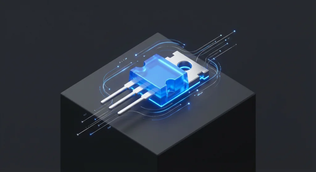
Matching networks are generally composed of lossless reactive elements, such as inductors (L) and capacitors (C). These components do not dissipate energy; instead, they store and release energy, modifying the phase and magnitude of the impedance without attenuating the signal. Common configurations include:
- L-networks: Simple and narrowband, using one inductor and one capacitor.
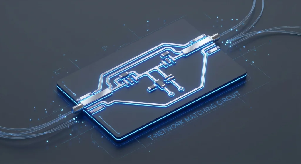
- Pi ($\Pi$) and T-networks: Offer greater flexibility and bandwidth, using three reactive components.
- Stubs: Short segments of open or short-circuited transmission line, used at very high frequencies where discrete components become ineffective.
An indispensable tool for matching network design is the Smith Chart. It allows visualization of complex impedances and their transformation through the addition of series or parallel components. Designers can plot the path from the load impedance to the desired impedance (typically the transmission line's characteristic impedance or the source's conjugate).
Design Processes and Steps
The process of designing an impedance matching network follows several systematic steps:
-
Impedance Characterization: The first step is to accurately determine the source ($Z_S$) and load ($Z_L$) impedances at the frequency(ies) of interest. This is often done using a Vector Network Analyzer (VNA), which measures S-parameters, with S11 (input reflection coefficient) being of particular interest.
-
Defining the Matching Objective: The most common goal is to achieve a conjugate match, where $Z_L$ is transformed to $Z_S^*$. If the source and transmission line have a real impedance of $Z_0$ (e.g., $50 \Omega$), the objective is to transform $Z_L$ to $Z_0$.
-
Selecting the Matching Network Topology: Based on the frequency range, desired bandwidth, Q-factor, and space constraints, a topology (L, Pi, T, stub) is chosen. L-networks are ideal for narrowband applications, while Pi and T-networks offer more control and bandwidth.
-
Calculating Component Values: Several methods can be used to calculate the exact values for inductors and capacitors:
- Graphical Method (Smith Chart): The designer plots the path from the load impedance to the target impedance, adding series reactances or parallel susceptances until the center of the chart (normalized $Z_0$ impedance) is reached.
- Analytical Method: Specific mathematical formulas are used for each L, Pi, or T network topology, often simplified for purely resistive cases or with a predetermined Q-factor.
- Simulation Software: Tools such as Keysight ADS, Ansys HFSS, or LTspice allow simulating the matching network's behavior and optimizing component values for desired performance.
-
Implementation and Tuning: Once the values are calculated, the network is built using discrete components (SMD capacitors and inductors) or distributed elements (microstrip stubs). During the prototyping phase, it is common to perform fine-tuning with a VNA, replacing components or using variable capacitors and inductors to achieve the best possible match.
-
Verification: The S11 (or VSWR) of the implemented network is measured to ensure that the reflection coefficient is minimal at the operating frequency(ies) and that power is transferred efficiently.
Key Parameters and Future Outlook
The performance of an impedance match is evaluated using several key parameters:
- Reflection Coefficient ($\Gamma$ or S11): Indicates the fraction of reflected power. An S11 of 0 dB means total reflection; an S11 of -20 dB means only 1% of the power is reflected.
- VSWR (Voltage Standing Wave Ratio): A VSWR of 1:1 indicates a perfect match (no standing waves). Values greater than 1:1 indicate reflection.
- Return Loss (RL): Is $20 \log_{10} |\Gamma|$. Measures losses due to reflection.
- Insertion Loss (IL): Measures the signal attenuation through the matching network. In ideal passive networks, it should be 0 dB.
- Bandwidth: The range of frequencies over which the matching network maintains acceptable performance.
Looking to the future, impedance matching remains an active area of research, especially with the rise of new technologies:
- 5G and mmWave Systems: Higher frequencies and wider bandwidths require more sophisticated matching networks, often utilizing distributed components integrated into the substrate (e.g., microstrip or stripline) instead of discrete components.
- IoT and Low-Power Devices: There is a drive for miniaturization and low-cost, low-power matching networks for wireless communication modules.
- Active and Tunable Matching Networks: Using varactors or RF switches, networks can be created that dynamically adapt to environmental impedance changes (e.g., an antenna in different environments) or different frequency bands, continuously optimizing power transfer.
- Artificial Intelligence and Machine Learning: AI techniques are being explored for the automated design and optimization of complex matching networks, particularly in scenarios with multiple variables and constraints.
Impedance matching is and will remain a fundamental pillar in the design of communication and signal processing systems, ensuring that hardware operates with maximum efficiency and reliability.
📊 Practical Example
Real-World Scenario: Antenna Matching for a 2.4 GHz IoT Module
Problem: A Wi-Fi module (source) with an output impedance of $Z_S = 50 \Omega$ needs to be connected to a patch antenna whose input impedance, measured at 2.4 GHz, is $Z_A = (30 - j70) \Omega$. The goal is to design a matching network to maximize power transfer and minimize reflections at 2.4 GHz.
Objective: Transform the antenna's impedance ($Z_A$) to the source's impedance ($50 \Omega$) using an L-network (two components).
Design Steps (using the Smith Chart as a conceptual guide):
-
Load Impedance Normalization:
- Normalize $Z_A$ with respect to the system impedance $Z_0 = 50 \Omega$: $z_a = Z_A / Z_0 = (30 - j70) / 50 = 0.6 - j1.4$.
- This point $(0.6, -1.4)$ is located on the Smith Chart, away from the center (which represents a perfect match $1.0 + j0$).
-
L-Network Topology Selection and Smith Chart Movement Strategy:
- To transform $z_a = 0.6 - j1.4$ to the center $(1.0 + j0)$, we can use an L-network with one series component and one parallel component.
- A common strategy is to move the point $z_a$ to a constant conductance circle ($g=1$) or a constant resistance circle ($r=1$), and then add a parallel or series component to reach the center.
- For this case, let's consider the path of series inductive and parallel capacitive components.
-
Component Calculation (Illustrative Method with Smith Chart and Formulas):
-
Step A: Add a Series Inductive Reactance ($L_{series}$):
- From $z_a = 0.6 - j1.4$, we want to move along the constant resistance circle $r=0.6$ by adding a series inductor (moving counter-clockwise on the Smith Chart) until the resulting impedance intersects the $g=1$ constant conductance circle (or its equivalent in the impedance plane, $R=Z_0$).
- An approximate intersection on the Smith Chart for $r=0.6$ and $g=1$ is $0.6 + j0.8$.
- The required inductive reactance is $X_{series} = 0.8 - (-1.4) = 2.2$ (normalized).
- Denormalizing: $X_{series} = 2.2 \times 50 \Omega = 110 \Omega$.
- At 2.4 GHz, the value of the inductor $L{series}$ is: $L{series} = X_{series} / (2\pi f) = 110 \Omega / (2\pi \times 2.4 \times 10^9 \text{ Hz}) \approx \mathbf{7.29 \text{ nH}}$
- The new normalized impedance is $z_{mid} = 0.6 + j0.8$.
-
Step B: Add a Parallel Capacitive Susceptance ($C_{parallel}$):
- For the next step, it's convenient to work with admittances. Convert $z{mid}$ to normalized admittance: $y{mid} = 1 / z_{mid} = 1 / (0.6 + j0.8) = (0.6 - j0.8) / (0.6^2 + 0.8^2) = (0.6 - j0.8) / (0.36 + 0.64) = 0.6 - j0.8$.
- We are now at point $(0.6, -0.8)$ in the admittance plane of the Smith Chart. We want to reach the center $(1.0 + j0)$.
- We need to add a parallel susceptance to cancel the imaginary part $-j0.8$. To do this, we add a capacitive susceptance $B_{parallel} = +j0.8$ (normalized).
- Denormalizing $B{parallel}$: $B{parallel} = +j0.8 \times Y_0 = +j0.8 \times (1/50 \Omega) = +j0.8 \times 0.02 \text{ S} = +j0.016 \text{ S}$.
- At 2.4 GHz, the value of the capacitor $C{parallel}$ is: $C{parallel} = B_{parallel} / (2\pi f) = 0.016 \text{ S} / (2\pi \times 2.4 \times 10^9 \text{ Hz}) \approx \mathbf{1.06 \text{ pF}}$
-
-
Matching Network Results:
- The matching network consists of a series inductor of approximately 7.29 nH followed by a parallel capacitor of approximately 1.06 pF (placed between the antenna and the 50 $\Omega$ line).
-
Verification and Tuning:
- Once the network is built with real components (which will have tolerances), it would be connected to a VNA. The S11 parameter would be measured. Very low S11 values (e.g., below -20 dB) and a VSWR close to 1:1 at 2.4 GHz would be expected. If necessary, fine-tuning of the components (e.g., with variable capacitors or by trimming inductor leads) would be performed to optimize performance.