How a BJT Transistor Works: Technical Guide
💡 Quick Tip
The Bipolar Junction Transistor (BJT) is a fundamental pillar of analog electronics, acting as either a switch or a signal amplifier. Unlike MOSFETs, which are voltage-controlled, the BJT depends on the current injected into its base to modulate a much larger flow between the collector and the emitter. Mastering its use involves deeply understanding the cutoff, active, and saturation regions to avoid overheating or signal distortion. It is vital to correctly calculate the base resistance using the Beta gain and Ohm's Law, ensuring the device operates efficiently and safely in any professional printed circuit board design in 2026.
Introduction to Bipolar Junction Transistors (BJT)
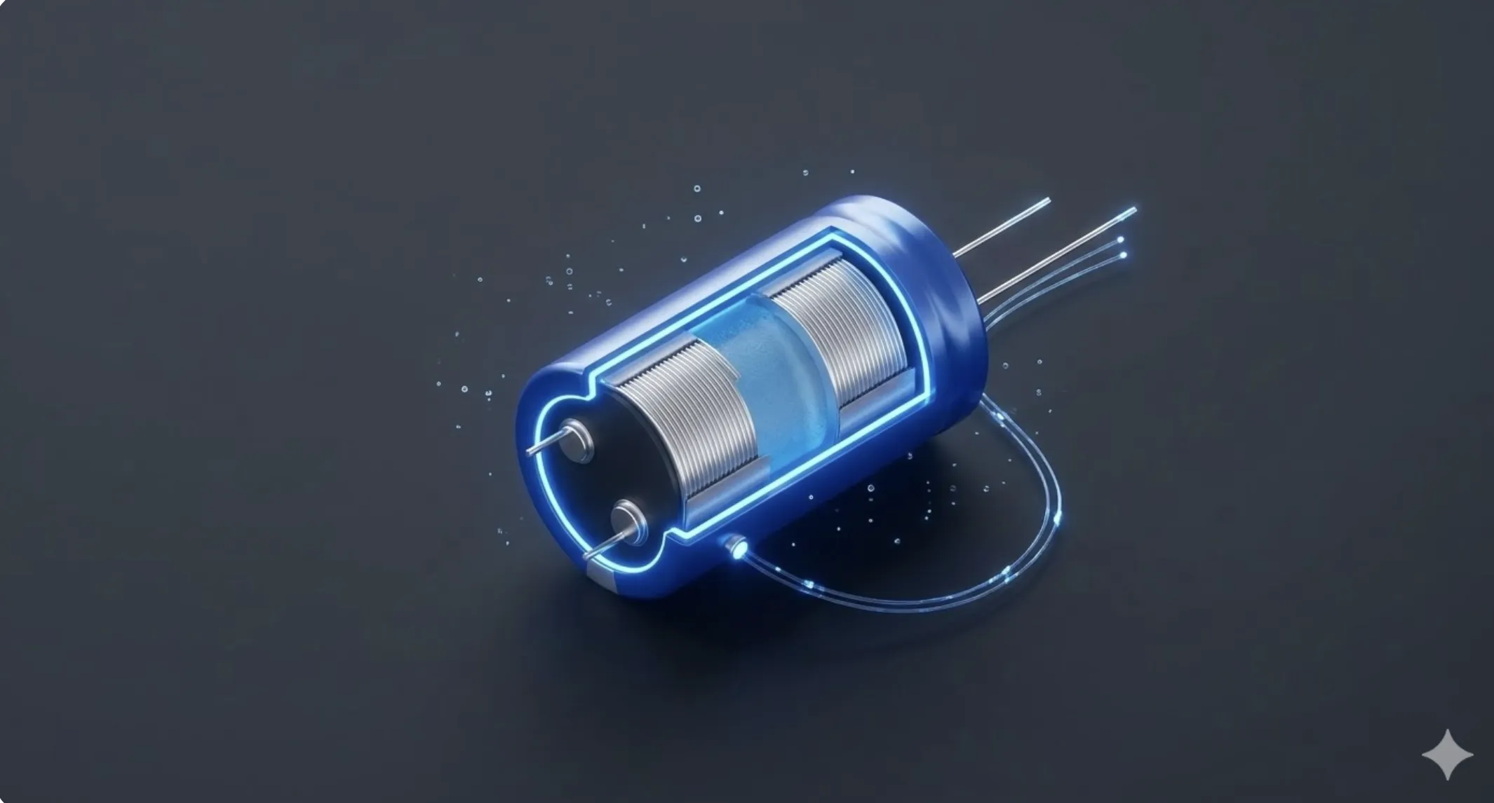
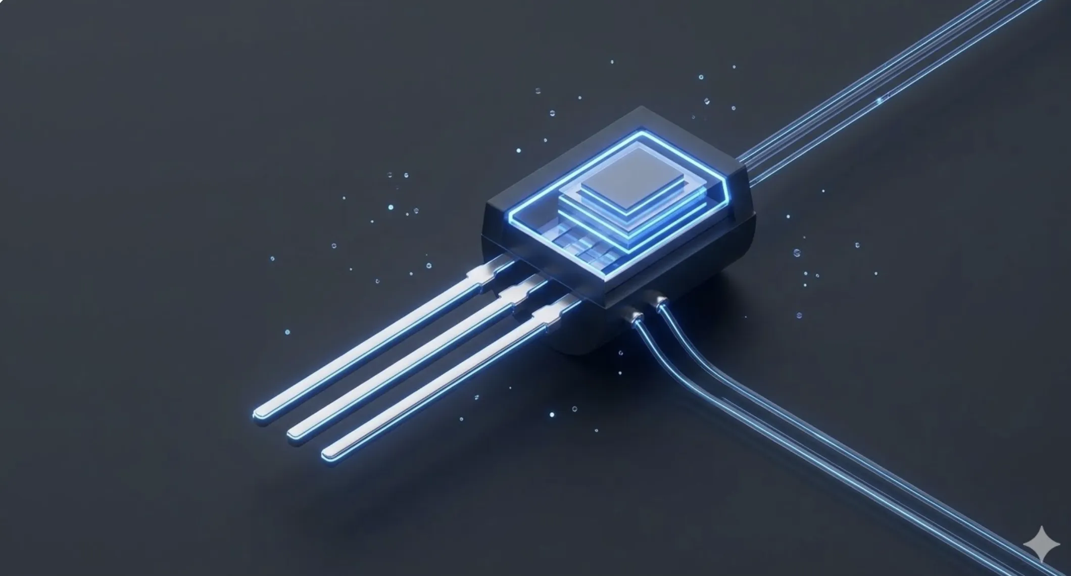
The Bipolar Junction Transistor or BJT is a fundamental semiconductor component in modern electronics. Its invention marked the transition from bulky vacuum tubes to the miniaturization of integrated circuits. A BJT is a three-terminal device consisting of the Base (B), Collector (C), and Emitter (E). The core physical principle involves the interaction of two PN junctions in close proximity, allowing a small current at the base to modulate and control a significantly larger current flowing between the collector and emitter.
Architecture and Types: NPN vs. PNP
BJTs are classified into two main types based on their doping structure:
- NPN Transistors: A thin layer of P-type material (the base) is sandwiched between two N-type layers (emitter and collector). These are the most common due to the higher mobility of electrons compared to holes, enabling faster switching speeds.
- PNP Transistors: An N-type layer is situated between two P-type layers. In this configuration, the main current flow is from the emitter to the collector when the base is pulled to a lower potential relative to the emitter.
Operating Regions
To use a BJT effectively in circuit design, one must understand its three operational states:
- Cut-off Region: The base current is zero ($I_B = 0$). The transistor behaves like an open switch, blocking current flow between collector and emitter.
- Active Region: This is the linear amplification zone. The collector current ($I_C$) is proportional to the base current, determined by the gain factor known as Beta (β) or $h_{FE}$. Here, $I_C = β cdot I_B$.
- Saturation Region: The transistor acts as a closed switch. Increasing the base current further does not increase the collector current, as it has reached the maximum allowed by the external circuit.
Critical Design Parameters
When designing with BJTs, engineers must account for power dissipation ($V_{CE} cdot I_C$) to prevent thermal runaway and ensure the collector-emitter breakdown voltage ($V_{CEO}$) is never exceeded.
📊 Practical Example
Real-World Scenario: Power Controller Design for Inductive Loads
Imagine you are designing an automation system for a smart greenhouse. You need to activate a 12V irrigation solenoid that consumes a constant current of 500 mA, but your controller is an ESP32 whose digital outputs only provide 3.3V and a maximum of 12 mA per pin. Attempting to connect the solenoid directly would destroy the microcontroller instantly. To solve this technical challenge, we will implement a power NPN BJT transistor, such as the TIP120, configured as a low-loss electronic switch.
Step 1: Data Sheet Analysis. First, we identify the critical parameters of the TIP120. Being a Darlington pair, it has an extremely high current gain (hFE), typically around 1000. This means that with a very small base current, we can control large loads. The maximum collector current ($IC$) is 5A and the maximum collector-emitter voltage ($V{CEO}$) is 60V, so our 12V/500mA load is well within the recommended 20% technical safety margins.
Step 2: Base Limiting Resistor Calculation ($R_B$). To ensure the transistor enters the saturation region (acting as a closed switch with minimal voltage drop), we must inject enough current into the base ($I_B$). We apply the formula: $I_B = I_C / hFE$. For 500mA, the theoretical current is 0.5 mA. However, to ensure saturation under any temperature condition, we apply an overdrive factor of 3, setting $I_B$ to 1.5 mA. Using Ohm's Law: $RB = (V{pin} - V_{BE}) / IB$. With $V{pin} = 3.3V$ and a saturation $V_{BE}$ for Darlington of approximately 1.4V, the calculation is: $(3.3 - 1.4) / 0.0015 = 1266 \Omega$. We select a commercial 1k$\Omega$ resistor for added safety, ensuring fast and full switching.
Step 3: Flyback Diode Implementation (Inductive Protection). When working with a solenoid, which is an inductive load, the BJT faces an invisible danger: counter-electromotive force. When the transistor turns off, the solenoid's magnetic field collapses, generating a reverse voltage spike that can exceed 100V, piercing the transistor's PN junction. We install a 1N4007 diode in parallel with the load, with the cathode towards the positive. This diode provides a low-resistance path for the stored energy to dissipate safely, protecting the integrity of the circuit.
Step 4: Thermal Management and Stress Testing. Although the TIP120 is robust, we calculate the dissipated power: $P = V_{CE(sat)} \cdot IC$. With a $V{CE(sat)}$ of 0.8V at 500mA, the power is 0.4W. Even though the TO-220 package can dissipate this in the air, for 24/7 industrial operation in a hot environment, we install a small aluminum heatsink. Finally, we verify with an oscilloscope that the rise and fall times of the signal are clean, confirming that our BJT works efficiently as the heart of the irrigation system.